Mo­dern Microsco­py

A microsco­pe is a ty­pi­cal tool to ana­ly­ze tiny struc­tu­res. Wi­de­ly used in sci­ence and in­dus­try, microsco­py is im­portant in re­se­arch of ty­pi­cal­ly small mo­dern de­vices and ob­jects. Be­cau­se of the on­go­ing mi­ni­a­tu­riza­t­i­on of se­mi­con­duc­tor and me­cha­ni­cal de­vices, the need for high re­so­lu­ti­on microsco­pes is still growing. It is our aim to im­pro­ve known microsco­py tech­ni­ques and re­se­arch new ones.

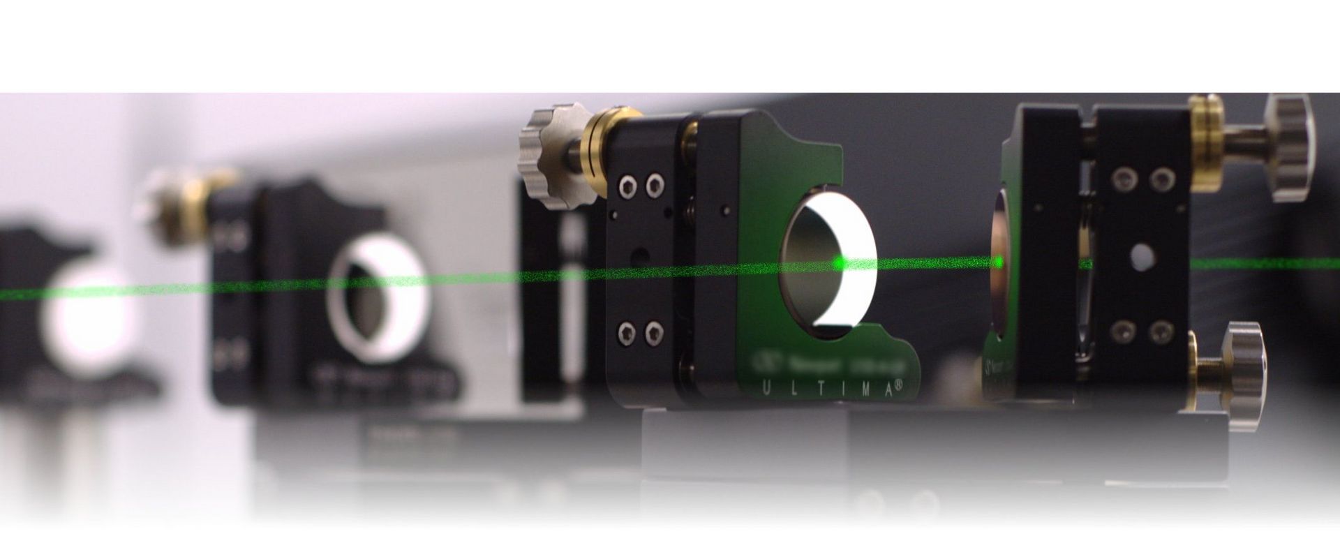
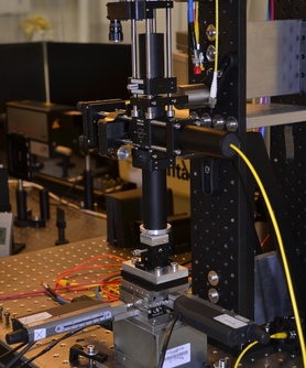
We rea­li­zed a fle­xi­ble con­fo­cal laser scan­ning microsco­pe (CLSM) to ana­ly­ze se­mi­con­duc­tor ma­te­ri­als in re­flec­tion and in micro-pho­to­lu­mi­nescence mode. The ca­pa­bi­li­ty to quick­ly chan­ge the laser sour­ces, ob­jec­tives and fil­ters al­lows a wide range of ex­pe­ri­ments with dif­fe­rent kinds of sam­ples. Cur­rent pro­jects im­ple­ment phase based me­thods to im­pro­ve the axial re­so­lu­ti­on, using syn­er­gy ef­fects of the re­se­arch pro­jects in the field of ho­lo­gra­phy and op­ti­cal co­he­rence to­mo­gra­phy (OCT). Using va­rious com­bi­na­ti­ons of pin­ho­le, ob­jec­tive and light sour­ce, the fol­lowing spe­ci­fi­ca­ti­ons can be ar­chi­ved:

  • 250nm la­te­ral re­so­lu­ti­ons
  • 50nm up to 100µm axial re­so­lu­ti­on
  • Laser sour­ces: Diode la­sers (405nm, 660nm and 1064nm), HeNe Laser and Ti:Sa Laser (700nm to 900nm)

Fi­gu­re 1: CLSM


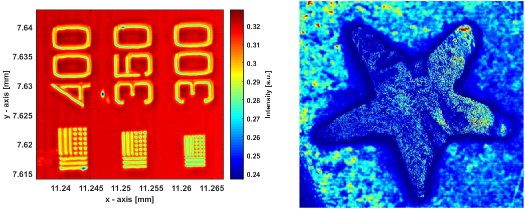
Fi­gu­re 2: Test chart with struc­tu­res of 400nm, 350nm and 300nm size

Fi­gu­re 3: Star on a 1 € coin

Fur­ther­mo­re, a con­trast en­han­ce­ment me­thod was de­ve­lo­ped which enables also high qua­li­ty ima­ging of struc­tu­res with a low height and low con­trast [1].

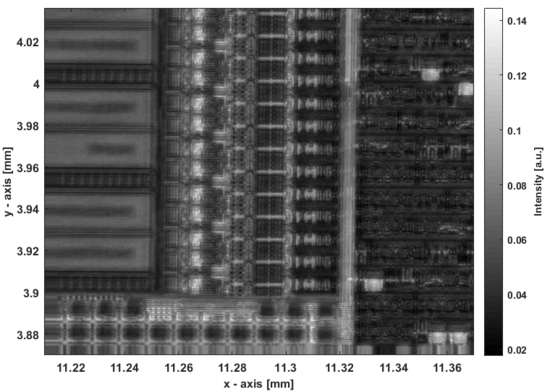
In the last years, we were able to im­pro­ve the mul­ti­modal ima­ging of bu­ried struc­tu­res and thus can for ex­amp­le me­a­su­re the in­te­gra­ted cir­cuits of a micro­con­trol­ler (see Fi­gu­re 4). In ad­di­ti­on to the re­flec­tion in­for­ma­ti­on of the con­fo­cal microsco­pe, op­ti­cal beam in­du­ced cur­rent (OBIC) can be used as a com­ple­men­ting con­trast me­cha­nism. In OBIC a laser in­du­ces car­riers in se­mi­con­duc­tor ma­te­ri­al which can be me­a­su­red as a cur­rent [2,3].

Fi­gu­re 4: Con­fo­cal image of bu­ried struc­tu­res of a micro­con­trol­ler me­a­su­red through the si­li­con sub­stra­te.

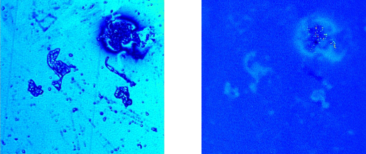
An im­portant sub­ject is the ana­ly­sis of se­mi­con­duc­tor ma­te­ri­als, es­pe­ci­al­ly the III/V se­mi­con­duc­tors for op­ti­cal in­te­gra­ted cir­cuits. The micro-pho­to­lu­mi­nescence mode al­lows spec­tral ima­ging in the range of 400nm to 1700nm.

Fi­gu­re 5: 200µm x 200µm se­mi­con­duc­tor samp­le in re­flec­tion mode

Fi­gu­re 6: 200µm x 200µm se­mi­con­duc­tor samp­le in pho­to­lu­mi­nescence mode

Re­fe­ren­ces:

  • [1] Lena Schnitz­ler, Mar­kus Fin­kel­dey, Mar­tin R. Hof­mann, Nils C. Ger­hardt. "Con­trast en­han­ce­ment for to­po­gra­phic ima­ging in con­fo­cal laser scan­ning microsco­py." Ap­p­lied Sci­en­ces 9(15) (2019): 3086.[1] Lena Schnitz­ler, Mar­kus Fin­kel­dey, Mar­tin R. Hof­mann, Nils C. Ger­hardt. "Con­trast en­han­ce­ment for to­po­gra­phic ima­ging in con­fo­cal laser scan­ning microsco­py." Ap­p­lied Sci­en­ces 9(15) (2019): 3086.
  • [2] Mar­kus Fin­kel­dey, Lena Gö­ring, Falk Schel­len­berg, Cars­ten Bren­ner, Nils C. Ger­hardt, Mar­tin R. Hof­mann. "Mul­ti­modal backsi­de ima­ging of a micro­con­trol­ler using con­fo­cal laser scan­ning and op­ti­cal-beam-in­du­ced cur­rent ima­ging." Proc. SPIE. 10110, Pho­to­nic In­stru­men­ta­ti­on En­gi­nee­ring IV, 101101F. (Fe­bru­ary 20, 2017).
  • [3] Lena Gö­ring, Mar­kus Fin­kel­dey, Falk Schel­len­berg, Cars­ten Bren­ner, Mar­tin R. Hof­mann, Nils C. Ger­hardt. "Op­ti­cal me­tro­lo­gy for the in­ves­ti­ga­ti­on of bu­ried tech­ni­cal struc­tu­res." tm-Tech­ni­sches Mes­sen 85(2) (2018): 104-110.

Fur­ther Re­fe­ren­ces:

  • Webb, Ro­bert H. "Con­fo­cal op­ti­cal microsco­py." Re­ports on Pro­gress in Phy­sics 59.3 (1996): 427.
  • Koukou­ra­kis, Nek­ta­ri­os, et al. "Axial scan­ning in con­fo­cal microsco­py em­ploy­ing ad­ap­ti­ve len­ses (CAL)." Op­tics ex­press 22.5 (2014): 6025-6039.

Col­le­agues:

Postal Address

Ruhr-University Bochum
Faculty of Electrical Engineering
and Information Technology
Photonics and Terahertz Technology
Postbox ID 16
Universitätsstraße 150
D-44801 Bochum

Contact

Office  
Room: ID 04/327
Te­l.: (+49) (0) 234 32 - 23051
Fax: (+49) (0) 234 32 - 14167
E-Mail: ptt+office(at)rub.de
RUB campus map & travel instructions

Chair Holder

Prof. Dr.-Ing. Martin Hofmann
Building: ID 04/329
Te­l.: (+49) (0) 234 32 - 22259
Fax: (+49) (0) 234 32 - 14167
E-Mail: martin.hofmann(at)rub.de

To Top