"Do not always take the mapped path It only leads you to where others have already walked."
Alexander Graham Bell
2D materials are a relatively young class of materials that consist of very thin, ideally monolayer, but still crystalline layers. A special feature is that different layers can be combined here even if their crystal lattices are not adapted. However, on the other hand, interface effects generally dominate the properties of layer stacks. This gives rise to many new questions from the production of large-area, monolayered layers, but especially from the targeted structuring of such thin layer stacks, which is essential for functional elements such as transistors or sensors and can only be solved with new technologies.
2D electronics / sensors have become transparent, flexible and biocompatible. The technology for this highly topical field of microelectronics based on 2D materials does not yet have the degree of maturity required for industrial mass applications.
Working in this field requires close interdisciplinary cooperation with chemists and plasma technology experts in order to research monolayer-precise, large-area additive and subtractive processes for 2D materials and to use them for innovative components and microsystems. Since the properties of 2D materials are closely linked to their crystal structure, the number of atomic layers, the morphology, the orientation, the interfaces and the doping, they can be configured in a variety of ways with regard to their mechanical, electrical and optical properties.
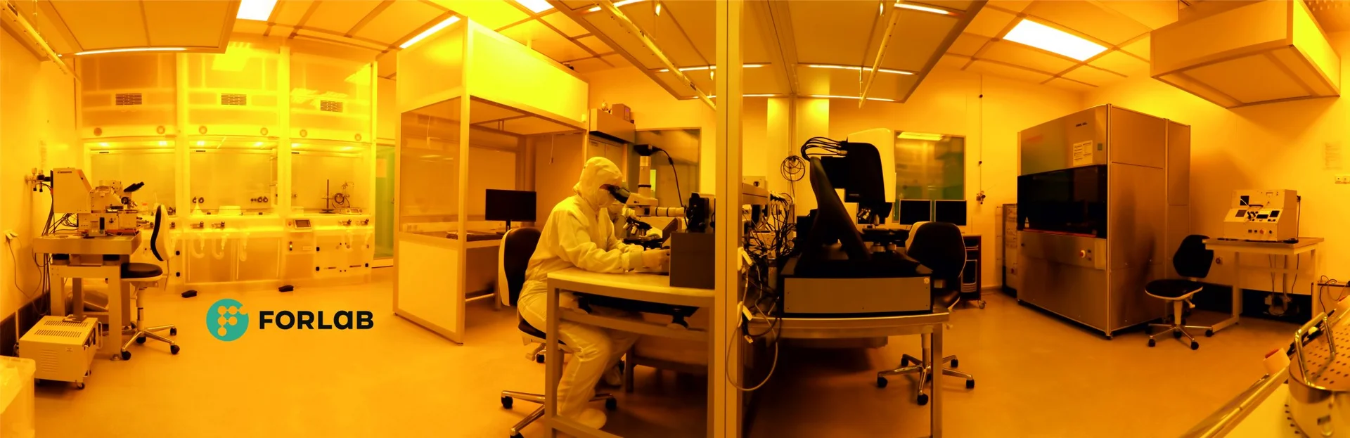
This work is based on a high-performance research infrastructure with innovative system technology in order to be able to process the highly sensitive layers continuously in a vacuum.
The basis for this is laid by the BMBF Research Laboratory Microelectronics Bochum for 2D electronics ForLab PICT2DES. It is one of 12 research laboratories in Germany. The subject matter is a process-integrating cluster tool for up to 200 mm substrates, which atomic layer deposition (ALD), atomic layer etching (ALE), plasma-assisted vapor deposition (PECVD) and reactive ion etching (reactive ion etching, RIE) combined with in-situ plasma diagnostics in one device, without breaking the vacuum during transfer between the processes. The aim is to develop novel electronic systems based on 2D integration that open up market segments such as flexible microelectronics, highly sensitive sensors or microfluidic systems.
The video about the ForLab site in Bochum and further information can be found on the following websites:
ForLab Website: https://www.forlab.tech/ueber-forlab/forlab-pict2des/
LinkedIn: https://www.linkedin.com/feed/update/urn:li:activity:6971039233461387264
Facebook: https://www.facebook.com/ForLabDeutschland/
As part of the DFG priority program „High Frequency Flexible Bendable Electronics for Wireless Communication Systems” FFlexCom, SPP 1796, it is about the realization of the first completely flexible, integrated thin-film electronics for wireless communication and its high-frequency properties. In order to achieve frequencies in the low GHz range, innovative material classes are used which, in addition to high mobility, offer sufficient mechanical stability. Together with the group for inorganic chemistry (Prof. Dr. Anjana Devi) the fascinating material class of Ütransition metal dichalcogenides and their application in flexible, pliable electronics is being researched. The transition metal dichalcogenides show a high degree of transparency, a significantly higher conductivity and high mechanical stability compared to the organic and metal oxide semiconductors.
As part of the BMBF-funded ForMikro Project „Research into new, flexible sensor systems based on two-dimensional material systems“ FlexTMDSense, a consortium of four groups from the RUB (microsystem technology, chemistry of inorganic materials, general electrical engineering and plasma technology, laser application technology) and the Fraunhofer Institute for Microelectronic Circuits (IMS ) Duisburg. The project is accompanied by six industrial partners. The aim is to manufacture first functional models of flexible sensor systems (gas sensors and pH sensor systems) on 200 mm substrates on the basis of 2D materials and building on the findings of basic research.