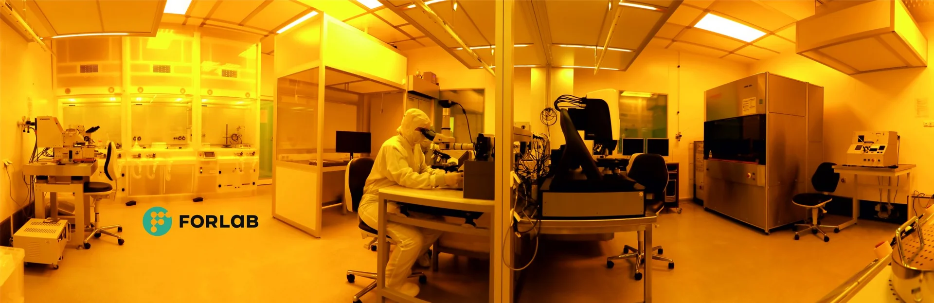
OPTICAL MICROSYSTEMS
Knowing is not enough, one has to apply; it is not enough to want, you have to do too."
Johann Wolfgang von Goethe
Optical microsystems form a continuous focus of research activities. Starting with waveguide systems for sensors and optical communication technology to emitters and absorbers for long-wave infrared technology. The focus here is on dielectric waveguides, either based on (doped) SiO2 or in the infrared based on silicon, which is highly transparent over an extremely wide range above the band gap (minimal absorption coefficient) and has a high but constant refractive index of 3, 5.
By means of suitable etching, the silicon surface can be roughened in such a way that a kind of moth-eye effect makes the transition from the refractive index low-reflection.
This topic is being researched in the BMBF project PaSiC „silicon-ceramic hybrid substrate as an integration platform for photoacoustic and optical applications“ (project start: October 2020) in cooperation with Infineon. With an additional suitable coating with metals, however, the same surfaces can also be transformed into almost ideal absorbers or emitters for IR radiation.
In the field of optical communication technology, very different concepts for optical switches have already been researched, which are either based on the mechanical movement of waveguides or which use the influencing of the effective refractive index of a waveguide in an adiabatic branch. The refractive index can be changed either thermo-optically (EU project COBNET, carried out at the University of Dortmund) or by dielectric switching of liquid jacket media (EU project SWIFT, carried out at TU Ilmenau). Waveguides with a pronounced evanescent field in particular have been developed for this application.
Waveguides based on photonic crystals are currently being implemented as tags for localization as part of the MARIE Teilprojekts C12. The narrow-band, high-resonance waveguide sections with mode converters designed by the TU Darmstadt (subproject C09) are manufactured in highly resistive silicon and have a very high quality. For the second phase of MARIE, the use of Si-based waveguides is planned - albeit in a very broadband configuration, e.g. as a dielectric slotted waveguide for THz radiation. For this purpose, the parameters from the near and middle IR range can be scaled up to the larger wavelengths in the THz range, since the Si properties remain practically constant; it “only” changes the wavelength.