Equipment
Forschungslabor Mikroelektronik Bochum - ForLab Bochum
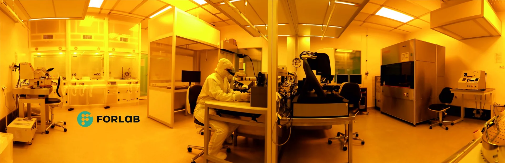
The „Forschungslabor Mikroelektronik Bochum“ - ForLab Bochum essentially includes the cleanroom of the Chair of Microsystems Technology at Faculty of Electrical Engineering and Information Technology (RUB) and provides essential basic technologies for microsystem technology and 2D semiconductor technology on substrates up to 200 mm.
- Link ForLab Website:
Mikroelektronikforschung an der Ruhr-Universität Bochum
- Downloadlink Terms of Use (pdf-File):
Nutzungsordnung des Gerätezentrums "Forschungslabor Mikroelektronik Bochum" - ForLab Bochum
Our Clean Room
")
")
")
")
")
")
")
")
")
")
")
")
")
")
")
")
")
")
")
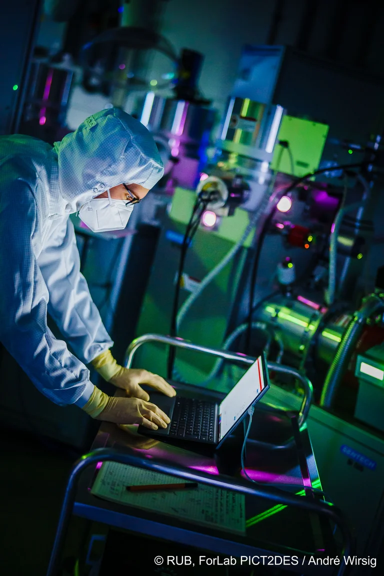
The chair for microsystems technology has facilities for the preparation of semiconductor micro- and nanostructures
These include, among others:
- Mask-Aligner, Heatpads, Oxidizing ovens, Plasma incinerator, Spin coater, Laser lithography system (structure widths > 600 nm), Scanning electron miscroscope / electron beam lithography system, Inert gas glove box with spin coater and Ozone Cleaner, Plasma etching machine (ICP-RIE), Evaporation systems, Wafer saws, Plasma coating system (ICPECVD), Tempering systems, Scoring device
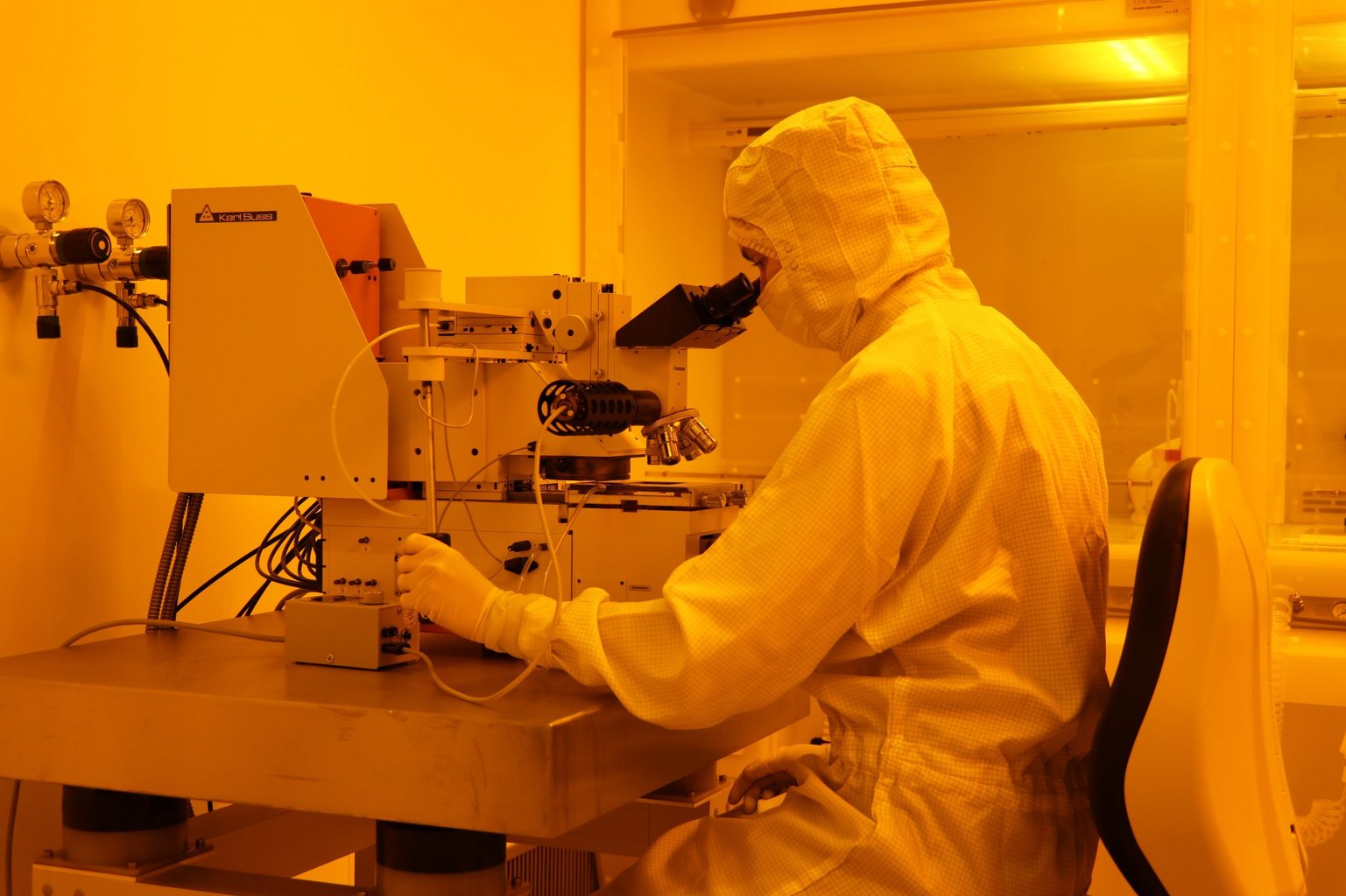
During the preparation, the components and systems are characterized with the following devices:
- optical miscroscopes, Ellipsometer, Interference microscope, Confocal microscope, Scanning probe microscopes (AFM, MFM)
Several cryostats (temperature range: 300 mK to 500 K) and electromagnets and superconducting magnets (up to 17 T) are available for magnetic field-dependent and temperature-dependent measurements. The electrical characterization is carried out using semiconductor parameter analyzers, lock-in technology (up to f = 200 MHz) and capacitance-voltage measuring devices.