MICRO-NANO INTEGRATION
This topic forms one of the long-term, overarching focal points of our own research; since 2007 Prof. Dr.-Ing. Martin Hoffmann leads the technical committee 4.7 Micro-Nano-Integration of the VDE specialist society GMM.
In particular, it is becoming apparent that the integration of post-CMOS nanostructures on microelectronic wafers will also play a key role within the framework of the More-than-Moore strategy. Since modern microelectronic foundries are almost completely converted to 200 mm substrates, there is a need in this area to be able to handle 200 mm wafers at least in some core processes or at least be able to load them into the systems. A completely homogeneous structuring or even automated handling is not necessary for this, as it will initially be about feasibility studies. This also includes the new field of two-dimensional material systems, which is being worked on as a separate focus in micro-nano-integration.
With the help of microsystem technology, the integration of nanostructures in microsystems is now possible in a variety of ways, e.g. through suitable self-masked or externally masked plasma etching processes. For this purpose, among other things, an etching process for Si-Gras needles controlled by optical emission spectroscopy was researched, which forms the basis for self-organizing nanostructures. In combination with nanoimprint lithography (NIL) and atomic layer deposition (ALD), many applications can be addressed here that benefit from the extremely large surface-to-volume ratio of nanostructures. Applications that are currently in the foreground are Si grass with additional coatings for medical technology and biology (wetting and dewetting properties, questions of cell growth on nano-surfaces) and as infrared-optical interfaces with anti-reflective or highly emissive properties.
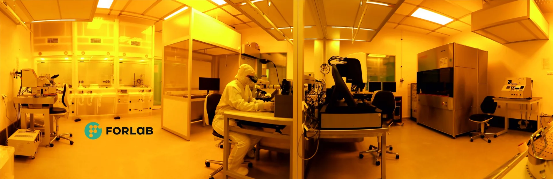
At this point there are also links within the RUB, in particular to the Center for Interfacial High Performance (ZGH), Research Department „Plasmas with Complex Interactions” and Materials Research Department. Micro-nano-integration is essentially based on the technologies listed above in order to make them accessible to small and medium-sized companies, supplemented by process technologies that are now available such as nano-imprint lithography (as an add-on to UV lithography) and electron beam -Lithography, modified deep Si etching and atomic layer deposition (ALD) as well as high resolution scanning electron microscopy.