Holographic Imaging
Two measurement techniques for topological measurements are currently applied at the group of Photonics and Terahertz Technology: photorefractive and digital Holography.
Basic Principles of Holography
The basic principle of holography is the superposition of two coherent beams creating an interference pattern, the so called hologram. If one of the beams has been reflected by an object, it is called object beam and contains the entire topographic information of the object. If this beam is superimposed with a plane reference beam onto a holographic material, a hologram is created in which the information of the object can be stored (Figure 1a). This information can be retrieved by again shining the reference beam onto the holographic material so that the object beam is recreated (Figure 1b).
")
Photorefractive Holography
Using a photorefractive material as holographic material is called photorefractive holography. When a broadband light source is deployed, the entire depth information can be saved for instance in a photorefractive crystal with only one shot [1,2]. An evaluation over all spectral components, which is similar to optical coherence tomography, enables the recovery of the depth information. The lateral resolution is defined by the size of the pixels of the camera and optics used optionally and lies in the µm range. It is however restricted to the diffraction limit. The axial resolution is dependant on the amount of the spectral components of the light source and is currently about 100 µm. The photographic image and the measured depth information of a sample are given in figure 2a and 2b.
")
Digital Holography
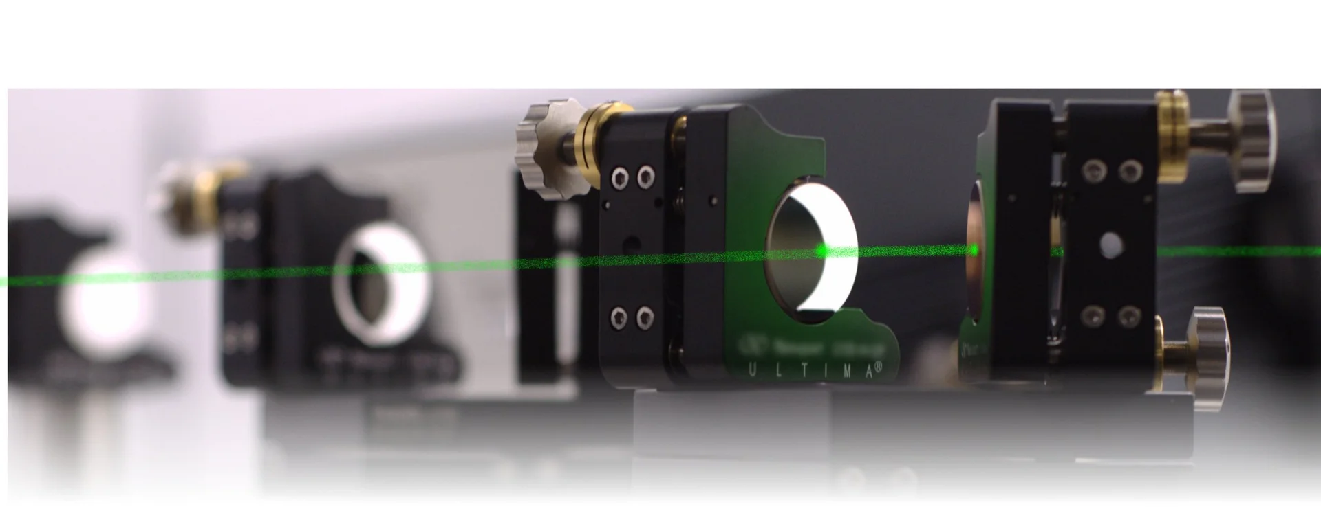
In contrast to photorefractive holography, there is no holographic material recording the hologram. A CCD- or CMOS Camera is instead used to save the interference pattern. A principle digital holography set-up is shown in Figure 3a.
")
Figure 3a: Principle set-up of digital holography , O = object beam, R= reference beam
Amplitude and phase of the object beam are then numerically reconstructed in order to gain the object information. The lateral resolution is defined by the size of the pixels of the camera and optics used optionally and lies in the µm range. The axial resolution is in the range of 10 nm. A reconstruction of bond pads of a MOEMS structure (Figure 3b) is given in Figure 3c.
")
Digital holographic Microscopy
When expanding the digital holographic set-up by a microscope objective, both lateral and axial resolution can be increased. Furthermore, numerical amplitude and phase filters can be applied to the recorded data, so that filter effects like dark field microscopy can be carried out without adding further mechanical components to the set-up. A typical digital holographic microscopy set-up is shown in Figure 4.
")
Figure 4: Digital holographic microscopy, O = object beam, R = reference beam, MO = microscope objectiv
The amplitude and the phase reconstruction of a USAF test chart can be seen in Figure 5a and 5b respectively.
")
As the topographic structure of an object is encoded in the phase information, it can be numerically unwrapped. A three dimensional representation of the USAF test chart is shown in Figure 6. Differences in height between 10 and 400 nm can be reconstructed. Laterally, the resolution is restricted to the diffraction limit and is smaller than 2 µm.
")
Fig 6: 3-dimensional reconstruction of the testchart
Dual-wavelength scanning
Samples characterized by bigger differences in height, can be measured with the help of dualwavelength scanning. This technique uses two holograms at two different wavelengths. The phase difference of these two holograms is calculated representing a higher synthetic wavelength with which higher structures can be reconstructed. Figure 7 shows the reconstruction of 200 µm high metal steps, which was calculated with two holograms at wavelengths of 833 and 834 nm.
")
Figure 7: 3-dimensional reconstruction of step sample, recorded by dual wavelength scanning
Overview of Resolution of holographic Techniques
| Technique | Imaging area | Lateralresolution | Axial resolution(minimun) | Axial resolution(Maximum) |
| Photorefractive Holography | up to 25 mm² | dependant on size of pixel | 200 µm | 1,5 mm |
| Digital Holography | up to 25 mm² | dependant on size of pixel | 30 nm | 420 nm |
| Digital holographic Microscopy | 10 mm² to 0,1 mm² | up to 1µm | 10 nm | 420 nm |
| Dual-wavelength scanning | up to 25 mm² | up to 1 µm | 450 nm to 3,5 µm | 9 µm to 70 µm |
Reference:
- [1] Koukourakis, N., Kasseck, C., Rytz, D., Gerhardt, N. C., & Hofmann, M. R. (2009). Single-shot holography for depth resolved three dimensional imaging. Optics Express, 17(23), 21015-21029.
- [2] D. Grosse, N. Koukourakis, N. C. Gerhardt, T. Schlauch, J. C. Balzer, A. Klehr, G. Erbert, G. Tränkle, and M. R. Hofmann, “Single-shot holography with colliding pulse mode-locked lasers as light source,” in Proceedings of the International Quantum Electronics Conference and Conference on Lasers and Electro-Optics Pacific Rim 2011, (Optical Society of America, 2011), paper C835.
Self-referencing digital holographic microscopy
")
Many typical holographic microscopic setups generate a hologram by overlaying an object wave and a reference wave, which travel along different paths before they interfere with each other. The very high sensitivity of these systems, which is on the one hand responsible for the superior phase resolution, makes these systems also very sensitive to disturbances from the environment, e.g. thermal changes or mechanical vibrations.
One concept to overcome these stability requirements is the common-path interferometer. Instead of separate object and reference beams, here the reference is directly created out of the object beam. For this purpose, an object beam is divided into multiple orders. One of the orders is spatially filtered, which creates the reference, while the other order remains unfiltered. The interference of both orders creates the hologram. Since both object and reference travel along the same optical path, external disturbances influence both beams in the same manner. Therefore, they remain stable in relation to each other. Furthermore, since both object and reference have their origin in the object wavefront, small variations of the sample have no significant influence on the phase stability. This concept of self-referencing highly decreases the stability requirements of these systems. These systems are not only perfectly suited for online monitoring of samples or processes, but also well capable of investigating buried structures [3,4].
Reference:
- [3]: Finkeldey, M., Göring, L., Brenner, C., Hofmann, M., & Gerhardt, N. C. (2017). Depth-filtering in common-path digital holographic microscopy. Optics Express, 25(16), 19398-19407.
- [4]: Neutsch, K., Schnitzler, L., Sun, J., Tranelis, M. J., Hofmann, M. R., & Gerhardt, N. C. (2020, February). In-depth particle localization with common-path digital holographic microscopy. In Practical Holography XXXIV: Displays, Materials, and Applications (Vol. 11306, p. 113060A). International Society for Optics and Photonics.
Digital Holographic Microscopy using Lloyd's Mirror Interferometer
")
Based on the concept of self-referencing interferometry, another setup is the Lloyd's mirror interferometer. Instead of separating the object beam in order to create a reference, like in the common-path interferometer, here the beam remains undivided. Instead, the sample is located in a manner that only one half of the beam is influenced by the structures of the sample. The other half of the beam remains mainly unaltered and is used as reference. In order to overlay the one half with the other, a mirror is used, which "folds" the one part into the other and thus creates the interference hologram. This hologram can be reconstructed like an ordinary off-axis hologram and contains amplitude as well as phase information of the sample. The Lloyd's Mirror setup requires only a small number of optical components is very stable and compact [5].
")
Due to its imaging capabilities and high phase sensitivity, holographic setups are very suitable for the detection of small particles. This can be interesting for numerous applications, e.g. optical authentication in IT-security (optical PUFs), bio-medical imaging, contamination detection in manufacturing and pollution control.
Reference:
- [5]: Neutsch, K., Schnitzler, L., Kleemann, N., Hofmann, M., & Gerhardt, N. C. (2019, October) "Holographic imaging of particles using Lloyd’s mirror configuration". Face2Phase II, Delft, the Netherlands
- [siehe auch]: Chhaniwal, V., Singh, A. S., Leitgeb, R. A., Javidi, B., & Anand, A. (2012). Quantitative phase-contrast imaging with compact digital holographic microscope employing Lloyd’s mirror. Optics Letters, 37(24), 5127-5129.
Transmission digital holographic imaging with modified Mach-Zehnder Interferometer
For a wide variety of applications, the investigation of samples in the transmission geometry is preferred. With universality and flexibility in mind, a Mach-Zehnder interferometer remains a commonly used option in such cases. The latter is a classical two-beam interferometric system and commonly suffers from its high susceptibility to the ambient noise compared to the common-path solutions. In order to benefit from the Mach-Zehnder geometry and at the same time to address the stability issue, the basic configuration can be modified: each of the corner mirrors can be replaced with a Michelson-like add-on out of a beamsplitter and a mirror [6]. Such a solution is schematically shown in Fig. 11 (adapted from [6]). Hereby the system acquires a stable performance [7] with phase accuracy of just 0.69° [6] whereas the instrument enables investigation of different samples in terms of their optical thickness. The imaging optics in the sample area can be easily changed and compensated. Examples of applications for a such a system include high-resolution imaging of spatially-confined structures [6], in-depth allocation of the micrometer-scale particles [8], online monitoring of the refractive index evolution during the photo-chemical reactions [9], carrier concentration mapping in semiconductor samples [10], and many others.
")
Fig. 11. Schematic representation of the modified Mach-Zehnder Interferometer with a universal delay-line: 1 – light source for imaging/probing, 2 – single-mode optical fiber, 3 – collimator, 4,6,8 and 10 – beamsplitters, 5 – optional neutral density filter, 7 and 9 – mirrors, 11 –camera.
Reference:
- [6] V.R. Besaga, A.V. Saetchnikov, N.C. Gerhardt, A. Ostendorf, and M.R. Hofmann, "Digital holographic microscopy for sub-μm scale high aspect ratio structures in transparent materials," Optics and Lasers in Engineering 121, 441-447 (2019); doi: 10.1016/j.optlaseng.2019.05.007.
- [7] V.R. Besaga, A.V. Saetchnikov, N.C. Gerhardt, A. Ostendorf, and M.R. Hofmann, "Performance evaluation of digital holographic microscopy for rapid inspection," OSA Technical Digest, Digital Holography and Three-Dimensional Imaging, Th3A. 10 (2019); doi: 10.1364/DH.2019.Th3A.10.
- [8] V.R. Besaga, A.V. Saetchnikov, N.C. Gerhardt, A. Ostendorf, and M.R. Hofmann, "Near real-time digital holographic imaging on conventional central processing unit," Proc. 3SPIE 11056, 110562I (2019); doi: 10.1117/12.2526112.
- [9] V.R. Besaga, A.V. Saetchnikov, N.C. Gerhardt, A. Ostendorf, and M.R. Hofmann, "Monitoring of photochemically induced changes in phase-modulating samples with digital holographic microscopy," Applied Optics 58 (34), G41-G47 (2019); doi: 10.1364/AO.58.000G41.
- [10] V.R. Besaga, N.C. Gerhardt, and M.R. Hofmann, "Digital holography for evaluation of the refractive index distribution externally induced in semiconductors," Proc. SPIE 11306, 1130608 (2020); doi: 10.1117/12.2544160.
Colleagues: