Wafer characterisation
")
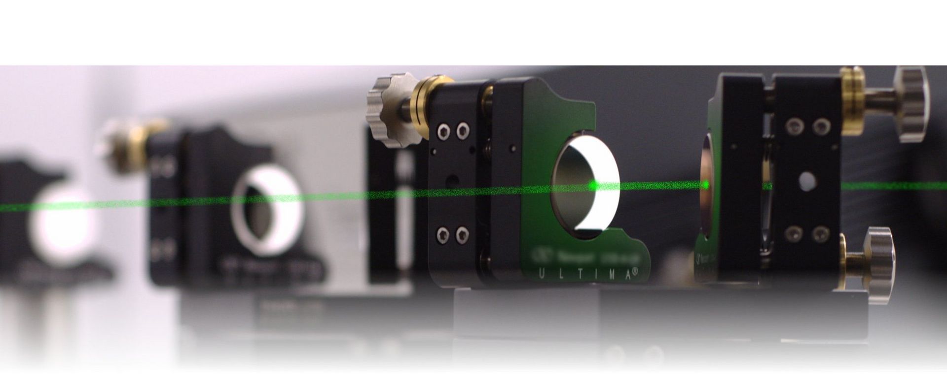
One challenge in Terahertz spectroscopy is the independent determination of refractive index and geometrical thickness of a given sample. This can be solved for semiconductor wafers by making use of the etalon effect induced by the plane parallel surfaces:
In a first step the frequency dependent transmission is measured. This could be done by tuning the beat frequency emitted by a dual mode Y-Laser [Link zu Y-Laser]. Extracting the envelope and performing a mean square error optimization to the theoretical etalon transmission will then result in n and d without any further sample knowledge.
Reference:
- N. Surkamp u. a., „Current tuned slotted Y‐branch laser for wafer thickness measurements with THz radiation“, Electronics letters, Bd. 57, Nr. 24, S. 936–938, Sep. 2021, doi: 10.1049/ell2.12314.
Colleagues: